|
Agile Circuit Co., Ltd
|

pcb design pcb layout PLC pcba assembly
| Payment Terms: | T/T,L/C,D/P,WU;Paypal |
| Place of Origin: | Guangdong, China (Mainland) |
|
|
|
| Add to My Favorites | |
| HiSupplier Escrow |
Product Detail
China PCB Design
Board Circuit Layout
PCB manufacture and assembly turnkey service
Remote Controller PLC PCBA Assembly
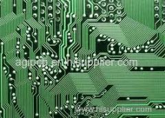
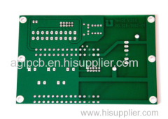
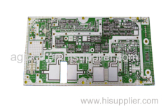
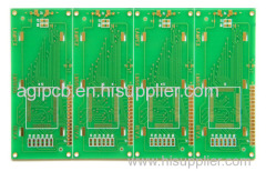
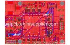
China PCB Design Board Circuit Layout for Remote Controller PLC PCBA Assembly
Quik Details:
4 Layers remote controller circuit boards
4 Output and input interface
Customized PCB boards specification
Low cost PLC solution replacement
Remote controller used in mitting system
PCB desgin and layout
Wireless communication devices, wireless base station etc.
Optical network transmission equipment, SDH, DWDM equipment etc.
Data communication equipment, high-end routers, LAN SWITCH, ADSL, etc.
Advanced computing devices,servers, motherboards etc.
Multimedia electronic devices TV, HDTV, DVD, DVB, LCDTV, PDP, LCOS, DLP
High-power switching power supply products, household appliances, computers, communications, switching power supply PCB design etc.
Power electronic equipment, inverter, UPS, industrial power etc.
Control Board, industrial PCB design series ect
Lighting Controls, LED light, Searchlights, Progressive Meters, Progressive Systems, Bingo Hall Management Systems, Electronic Systems Equipment, Pull-tab Equipment, Satellite Systems ect.
PCB Design
PCB Layout Design
PCB Circuit Reverse Engineering
PCB Fabrication
Prototypes PCB/Production
Rigid PCB manufacturing
Aluminium circuit board fab
Maximum Layers: 20 layers
Blinded and Buried Vias Supported
Minimum BGA pin-pith: 0.5mm
High Speed Differential Signal:10 GHz
Minimum Routing Width and Separation: 4mil
Minimum Via Hole Size: 8mil (4mil Laser Drill)
Short lead time. Our design team has sufficient experience in PCB design as well as strong manufacturing background. DFM allows us to do right. Our partnership factory also provides us great support for our commitment to short lead time.
High quality assurance .Standard PCB design flow, perfect quality assurance system, advanced manufacturing and testing equipment to provide excellent quality assurance.
Reduce the cost balance customer needs and manufacturing constraints, optimize PCB design to save time and money for customer.
Strong technical support. We can share success examples of manufacturing group members in their respective areas, and achieve the latest information for use, providing customers with more value.
PCB Design for Cost-down consideration
PCB Design process optimize
Design for Manufacturing, Design for Test, Design for Assembly (DFM, DFT, DFA)
High -density , blind and buried vias PCB design (High Density, B / B PCB design)
Thermal consideration in PCB design
Innovative PCB design method and technology
PCB stack up design optimization program
Signal Integrity simulation & analysis
EMC in PCB board design
Power Integrity analysis
PCB design power handling skills
PCB collaborative design team
Introduce new PCB layout & Simulation
Schematic
Netlist
Bill of Materials
Board Size an Boat shape
Preferred Number of Layers
Desired Lead Time
What percentage of the board is to be hand-routed versus auto-routed
special routing instructions
Our PCB layout design applications:
Description:
We are one stop PCB solution company from China. Our service includes PCB design, PCB layout, PCB manufacturing and assembly. We have PCB design divistion, PCB technical test dept., purchasing dept. OEM/ODM dept., research & development dept. and so on. PCB design dept. is with tens of professional designer who have been engaged in hard and soft ware more than 10 years. We could meet customer's requirement on PCB layout design, PCB copy, PCB schematic diagram, BOM, sample to medium manufacturing, technical support in single layer board, double sided PCB board, Multilayer PCB, high frequency PCB and so on.
PCB service we provide:
PCB Layout Design Spec.
Our PCB board design advantages:
Our technical advantages:
PCB Layout Design Quote Requirements
Didn't find what you're looking for?
Post Buying Lead or contact
HiSupplier Customer Service Center
for help!
Related Search
Pcb Layout
Pcb And Pcba
PCB Assembly
Led Pcb Assembly
Contract Pcb Assembly
Prototype Pcb Assembly
More>>
Find more related products in following catalogs on Hisupplier.com
Company Info
Agile Circuit Co., Ltd [China (Mainland)]
Business Type:Manufacturer, Distributor/Wholesaler, Service
City: Shenzhen
Province/State: Guangdong
Country/Region: China (Mainland)